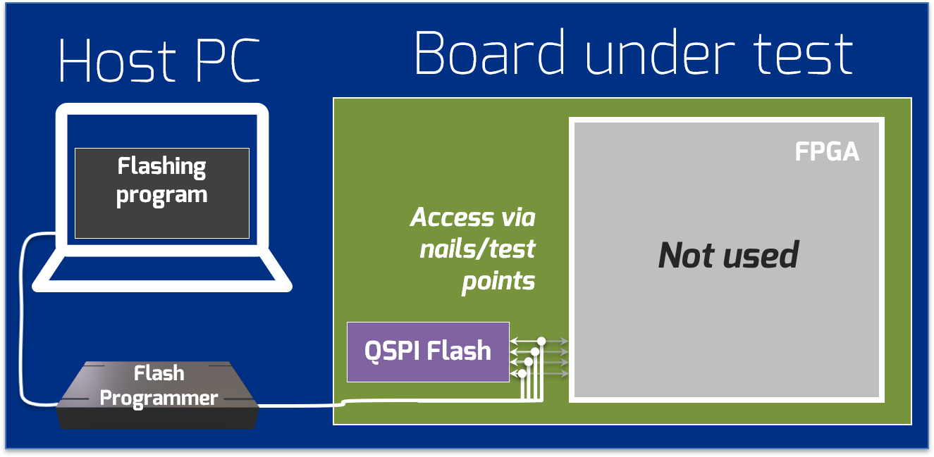
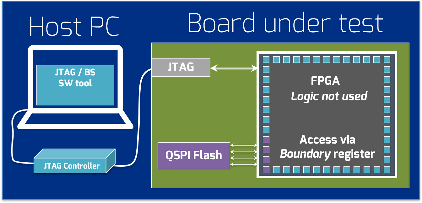
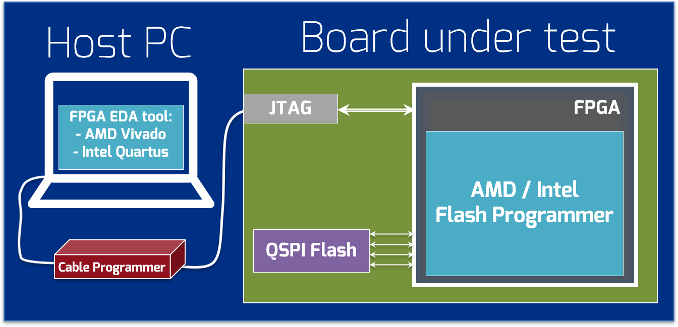
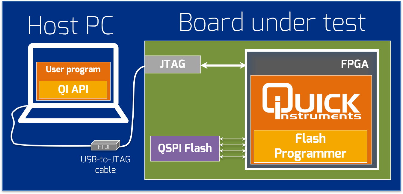
In-system Flash programming is an inevitable step during the manufacturing of an FPGA-based product. Most modern FPGAs lose their configuration after the power cycle. Therefore, a non-volatile memory device (normally QSPI flash) is placed on the PCBA to provide a boot source for the FPGA. During PCBA production, this flash memory must be written with a target configuration image (application firmware).

Standard Industry Practices: Pros and Cons

Let's study the common ways that are widely used at EMS factories. It is possible to distinguish three approaches:
  • Using an external Flash Programmer
  • Via Boundary Scan
  • FPGA-IP-based programming
*Don't miss the comparison table at the end of this article!

External In-System Programming

Flashing using an external programmer
Many companies provide dedicated hardware boxes that can access the flash on a board via test points. These programmers are optimized for speed, support automation features, and batch processing capabilities, which is especially important in high-volume production environments.

The key shortcoming of such a programming solution is a high NRE cost as a fixture with a bed-of-nails is required. Also, physical connections may have signal integrity issues, they are prone to mechanical damage and require regular maintenance.

Boundary Scan

Programming via Boundary register cells
Boundary Scan (BS) was introduced back in 1990 to overcome the problems of bed-of-nails. This non-intrusive technology with a much simpler connection via the JTAG port and Boundary register of FPGA is often used to program Flash.

However, the speed of BS is very limited. The growing size of FPGAs (and corresponding bitstreams that need to be programmed) turns Flash programming with Boundary Scan into a very time-consuming task. Quite often programming takes minutes but it can also last hours in the worst cases.

FPGA-IP-based Programming

Flash In-System Programming using FPGA logic
This approach solves the BS slow speed problem as instead of the Boundary shift register, the FPGA IP is used to communicate with a Flash device. The JTAG bus is used only for FPGA bitstream loading and for transferring flash programming data from the test station into IP.

Most FPGA engineers use this way of flash programming while they are developing projects with FPGA EDA tools (Vivado / Quartus / Radiant / Libero / Efinity). However, when the Flash programming should be done at the production facilities (by EMS company), it has to be automated and combined with other board-level tests. Occupying the JTAG port and using EDA tools only for Flash programming is inefficient.

This is the reason why all major JTAG / Boundary Scan vendors provide their own equivalent programming solutions: It should be noted, that all these vendors (besides Göpel) still require FPGA EDA tools (installed and licensed) to compile the programmer for the particular FPGA. Additionally, quite costly proprietary hardware (JTAG controllers) is necessary to use their programming solutions.

Testonica's Flash Programmer

Simple hardware, same high-speed programming (3Mbps)
QI Flash Programmer also uses the FPGA-IP-based approach. It delivers superior performance while having extremely modest requirements for test hardware. Even an inexpensive (50€) USB-to-JTAG cable (such as Digilent HS-3 or FTDI C232HM-DDHSL) will be sufficient to write a flash image in a matter of seconds.

Among other nice features, the QI-based solution includes several smart techniques such as checksum-based flash content verification and in-FPGA Flash blank check that boosts the performance of ISP to the level unreachable by conventional in-system and external programmers. When running on a simple USB cable, the effective throughput reaches 3Mbps for programming and up to 100Mbps for checksum-based verification. Those figures will go higher if a more advanced JTAG driver is used.

Just like all other instruments of the Quick Instruments framework, the Flash Programmer is well-suited for production environments. When combined with other QI instruments, flash programming can be employed along with or directly after the product test phase.

ARTY-S7 Demo

In our previous newsletter's edition, we described the standard QI application workflow based on the Arty-S7 board taken as a platform for a demo. The same steps are also required for the Flash Programmer. Testonica needs to know the pinmap between the FPGA and the target Flash to compile the FPGA-based instrument. For the Arty-S7 board, this excerpt is enough:
Page 6 of Arty-S7 schematic
QI Flash Programmer is easy to use and it supports many types of flash devices out-of-the-box via the built-in user-expandable flash model library. The Python code for the Programmer is pretty short and intuitive:
Python script for programming and verification

Programming Time Comparison

We did an experiment and programmed a sample binary (1.42MB, with a modest 30% logic utilization ratio) generated by Vivado into the IC7 (S25FL128) flash on the ARTY-S7 board. The results for the different techniques are presented below.

Table 1: Time required to program 1.42MB image into Arty-S7 SPI flash
Technology*
IP Loading
Program
Verify
Performance
Boundary Scan
-----
11m 31s
17m 44s
0.0065 Mbps
AMD Vivado Programmer
1.0 s
25.6 s
4.3 s
0.37 Mbps
Göpel's ChipVORX
1.0 s
2.5 s
2.0 s
2.06 Mbps
QI Flash Programmer
1.0 s
4.0 s
0.05 s
2.25 Mbps
*JTAG TCK speed was set to 30MHz in all cases
As expected, Boundary Scan was the slowest technology for programming. It took almost half an hour to program a relatively small firmware image. Vivado was 57x faster than BS but still, it showed a modest (although exactly as expected) result. This programming speed is enough for the prototype validation phase but as AMD itself claims "it is not intended for high-volume production programming". Göpel's ChipVORX demonstrated very good performance and taking into consideration that this technology comes off-the-shelf (no FPGA EDA tools required, the FPGA instrument is supplied with their SW) has a very promising fit-for-function performance.

Even so, the QI Flash programmer was still slightly faster than ChipVORX, 6x faster than Vivado, and 346x faster than Boundary Scan. Its performance is similar to what External In-System Programmers provide. At the same time, Quick Instruments has a set of unique features over external instrumentation:
  • No need for test points and nails, no signal integrity issues
  • Almost no price for a duplicate (only the price of a USB-to-JTAG cable)
  • No need for maintenance or calibration, can’t be outdated
  • Easier logistics: Instruments can be sent over email, copied, and backed up
Do you also have the ARTY-S7 board and want to try it yourself? Download the QI Runtime Demo version from here.
Want to try the QI Flash Programmer and try it on your FPGA board? Contact us and we will provide the demo instrument free of charge.