Diagnostic resolution is the KPI of test firmware
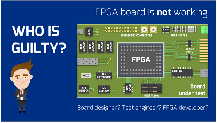
In one of our previous editions, we looked at typical ways of testing FPGA boards for production defects. In many cases, common test techniques like ICT, Boundary Scan, or Flying Probe cannot cover high-speed interfaces and components due to their technical limitations. The lack of dedicated technologies in the market forces product managers to make a simple decision: converting the mission-mode application firmware developed for the final product into a test firmware. Although this approach may harbor quality and logistic issues and require a great deal of conscious management, it has become a common way to close the coverage gap for FPGA-based products.
In reality, this task is usually borne by an FPGA firmware developer alone since nobody else (neither a board designer nor a test engineer) can cope with the complexity of FPGA handling and programming. So, there is simply no other choice but for the FPGA developer to become a superhero and in addition to his main responsibilities (often against his will) also work on test firmware that would need to check the hardware integrity of the board under test.
As a result, the inability to apply structural/electrical testing approaches, the board complexity and the ad-hoc firmware - altogether - intricates the board testing process and compromises quality. Even a small missed defect may result in the loss of a complete board.
Here is a typical story taking place when a board prototype of a new product is ready. The board designer brings the board to the FPGA developer so that he can check it out. The FPGA developer is happy to help as he also needs to verify that his code actually works on the target board. So, it's their common ground to test the developed product and make sure that the board and the application firmware are both working well.

But what usually happens is that the fresh prototype doesn't work stable or doesn't work at all and both the engineers are struggling hard to learn what goes wrong. At this stage, it is very hard to say, whether it is the board that has design issues or the firmware code that is buggy or it is just a configuration problem. Of course, both guys did their best during the development stage to ensure that both the board and the FPGA code are functioning well. Still, both tasks are very complex and hence error-prone. Moreover, it is not uncommon for a prototype board to have simple manufacturing defects like short circuits or opens complicating the troubleshooting challenge further. All in all, a myriad of problems might cause the prototype not working as expected. Eventually, both guys will have to engage into an intensive joint debug campaign and come up with a solution maybe after a few weeks or months.

The situation is even more problematic when the board designer and the FPGA developer belong to different supplier companies that do not cooperate closely enough with each other. Such cases may lead to significant delays in the product development process and missed deadlines. Both of them would benefit from somebody else jumping in and saying: "I can program your board with a correct-by-construction firmware, that you can use to simply verify your hardware separately from verifying the firmware code". The FPGA developer would also benefit from running his freshly developed code on a pre-verified and validated working board. This dream becomes a reality with Quick Instruments technology.
When the board has been validated, organizing mass production is the next task for the product manager. Now the test engineer comes into the game. Typically, it is his responsibility to develop a test program that will be executed for every assembled board on a production floor. The test engineer also turns to the FPGA developer asking to provide a test firmware that can be integrated into the test station.
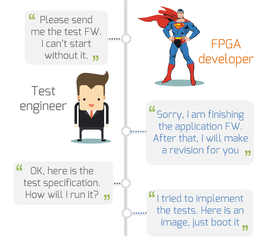
And this is another common cause of a contradiction. The key target for the FPGA developer is to make sure that his application firmware keeps working according to the product specification. For the test engineer, the task is different: he needs the test firmware to fail in case there is anything wrong with the board. So, the test engineer tries to make the system fail if only possible while the FPGA developer wants the system to keep working in all foreseen operating conditions. Hence, they face different challenges and normally do not understand each other as if they spoke different languages. The test engineer thinks in terms of defects like shorts and opens, a tombstone or a missing termination as well as many others that may occur during the PCB assembly process. The FPGA developer, on the contrary, has very little understanding or might even know nothing about these things that the test engineer has to address in his test program. Would it be a good test program in this case?

In the worst case, the FPGA developer will simply convert an application software into a test program that will simply light an LED, in the end, if everything works. If some tests fail - the LED will not light up providing prohibitively little diagnostic information for further troubleshooting. A pile of boards with unknown faulty status would then start to grow whereas nobody knows what exactly is wrong and how to repair them.
To sum up, there are certain drawbacks of using an application firmware for HW test:
Everything results in a lost test coverage inevitably leading to field returns, which is a problem for any company and requires improvements in the test development strategy.
We know very well that testing an FPGA board is a challenging task. FPGA development is an everyday routine in Testonica and we also help other companies bring up their new FPGA products. Talking to customers, we learn the difficulties that many test engineers and board designers are facing. Two decades of development work based on continuously collected experience have resulted in the Quick Instruments framework that addresses all these challenges providing better thoroughness in terms of testing at a faster execution performance as well as a shorter test development cycle. All in all, this approach improves the product quality and releases the FPGA developer so that he can focus on his primary responsibilities, which do not include test development.
The Quick Instruments framework can be reused throughout the complete cycle: from board design to test development to troubleshooting in production and aftermarket. Eventually, the product owner (OEM) becomes the ultimate beneficiary due to reuse.
Want to learn how Quick Instruments technology could save your everyday spendings on test and troubleshooting as well as help solving challenging quality-related issues for your FPGA-based product? Book a personalized demo!